DUV vs EUV: What’s the Real Difference in Chipmaking?
Introduction
As transistors shrink and chip complexity explodes, the tools used to etch microscopic patterns on silicon wafers must evolve. Two acronyms dominate this evolution: DUV (Deep Ultraviolet) and EUV (Extreme Ultraviolet). But what truly sets them apart?
In this article, we’ll break down the real technical and practical differences between DUV and EUV photolithography — and why EUV isn’t simply an upgrade, but a fundamental shift in how chips are made.
Wavelength: The Foundation of Resolution
At the heart of lithography lies one simple principle: shorter wavelengths can produce smaller features.
- DUV: Uses light at 248 nm (KrF) or 193 nm (ArF) wavelength.
- EUV: Uses light at 13.5 nm, more than 10x shorter.
This leap means EUV can pattern features under 10 nm, while DUV typically hits a limit around 40–20 nm (without complex tricks).
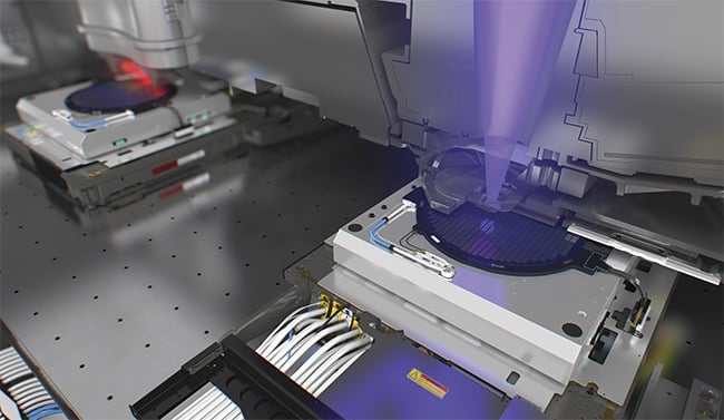
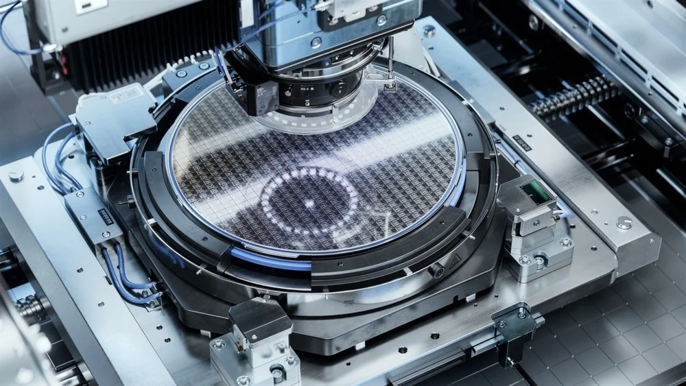
Light Source and Optics
| Feature | DUV | EUV |
| Light Source | Excimer lasers (ArF, KrF) | Plasma-generated EUV from tin droplets |
| Optics | Refractive (lenses) | Reflective (mirrors only) |
| Environment | Air (with nitrogen purge) | Vacuum required |
EUV’s extreme wavelength is absorbed by air and glass, so it must use mirrors in a vacuum — a major engineering leap.
Complexity and Cost
- DUV is mature and relatively affordable. Machines cost $20–50 million.
- EUV machines (from ASML) cost over $150 million, with massive support infrastructure.
Also, EUV masks are more delicate, and their inspection requires specialized tools. Even tiny defects can cause fatal chip flaws.
Resolution Enhancements
To keep DUV relevant at smaller nodes, engineers added techniques like:
- Immersion Lithography: Using water between lens and wafer to boost resolution
- Double/Quad Patterning: Exposing the wafer multiple times for finer features
These tricks add steps, time, and risk. EUV can skip many of them by printing features in a single pass.
Throughput: Speed vs. Precision
- DUV tools have high throughput and are faster for high-volume production.
- EUV started slower but is catching up — High-NA EUV will further improve throughput and resolution.
Use in Industry
| Node | Common Tech |
| 65–28 nm | DUV only |
| 20–10 nm | DUV + Multi-patterning |
| 7–3 nm | EUV (critical layers), DUV (supporting layers) |
| < 2 nm | High-NA EUV (future) |
Major players like TSMC, Samsung, and Intel now use EUV in volume production at advanced nodes.
Summary Table
| Aspect | DUV | EUV |
| Wavelength | 248/193 nm | 13.5 nm |
| Optics | Lenses | Mirrors |
| Medium | Air/Nitrogen | Vacuum |
| Resolution | ~20 nm limit | < 10 nm |
| Cost | $20–50M | $150M+ |
| Maturity | Very mature | Emerging/advanced |
Conclusion
DUV and EUV aren’t enemies—they’re collaborators. While DUV remains essential for many steps, EUV is the future of advanced chipmaking, enabling sub-5nm designs without endless process tricks.
Understanding their roles isn’t just for engineers. It’s key to grasping how the devices we use every day keep getting smaller, faster, and more powerful.
1 comment