What is Photolithography? A Deep Dive into the Heart of Chip Manufacturing
Introduction
Every smartphone, laptop, and high-performance computer chip in the world starts its life in a place you might not expect: under a beam of light. That light isn’t just any light—it’s a highly controlled ultraviolet (UV) beam used in a process known as photolithography. This process, essential to the creation of modern integrated circuits (ICs), is the hidden engine that powers our digital world.
But how does it actually work? And why is light such a powerful tool in crafting microscopic structures smaller than a virus? Let’s explore.
What is Photolithography?
Photolithography is a manufacturing technique that uses light to transfer geometric patterns from a mask onto a photosensitive chemical layer called a photoresist, which is applied to a silicon wafer.
Imagine trying to draw tiny electrical circuits with a flashlight and a stencil, where the light “draws” patterns onto a chemically treated surface. That’s photolithography in its simplest form.
These patterns define the transistors, wires, and structures that make up a microchip. With each layer, light helps sculpt an incredibly complex 3D circuit one slice at a time.
Why Use Light?
Why not use a laser, a needle, or even a microscopic pen? Because light offers unmatched speed, precision, and parallelism. Using a single flash, millions of transistors can be printed in a fraction of a second.
However, not all light is equal. Chipmakers use Deep Ultraviolet (DUV) and now Extreme Ultraviolet (EUV) light because their short wavelengths (193 nm for DUV and 13.5 nm for EUV) allow for finer details to be written.
In simple terms: the shorter the wavelength, the smaller the features you can etch.
Step-by-Step: How Photolithography Works
- Wafer Cleaning
- The silicon wafer is cleaned to remove contaminants that might interfere with the process.
- Coating with Photoresist
- A liquid photoresist is evenly spread across the wafer using spin-coating.
- There are two types:
- Positive photoresist: exposed areas become soluble.
- Negative photoresist: exposed areas harden.
- Soft Bake
- The wafer is baked at a low temperature to solidify the resist.
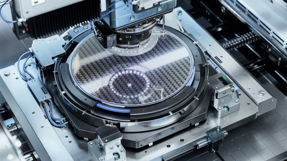
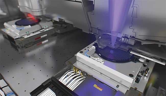
- Mask Alignment & Exposure
- A photomask containing the desired circuit pattern is aligned over the wafer.
- Ultraviolet light is projected through the mask, exposing specific areas of the photoresist.
- Development
- The wafer is placed in a chemical developer.
- Depending on the type of resist, exposed or unexposed regions are washed away, leaving the desired pattern.
- Etching
- The exposed parts of the underlying silicon (or other layers) are etched away using plasma or chemicals.
- Photoresist Removal (Stripping)
- The remaining photoresist is stripped off, leaving a precisely shaped pattern on the wafer.
Each step is repeated dozens (even hundreds) of times to create multi-layered chips.
Materials and Equipment
- Silicon Wafers: Pure, flat, crystalline bases
- Photoresist Chemicals: Light-sensitive polymers
- Photomask (or Reticle): A quartz plate with chrome patterns
- Stepper or Scanner Machines: Project UV light through the mask
- Etching Tools: Plasma or wet etch systems
One of the most advanced lithography machines today is made by ASML, capable of EUV lithography with nanometer-scale resolution.
Challenges in Photolithography
Photolithography has pushed physics to the limit. Some major challenges include:
- Diffraction Limits: Light tends to bend, especially at small scales, making it hard to print fine patterns.
- Overlay Accuracy: Aligning new layers perfectly over previous ones.
- Cost: EUV machines cost over $150 million each.
- Mask Defects: Any tiny error on the mask gets replicated on every chip.
Despite these challenges, innovation in optics, light sources, and materials continues to push the limits.
The Future: Beyond EUV
As we approach the 2nm node and beyond, even EUV may struggle. Researchers are exploring:
- High-NA EUV: Better optics for even finer resolution
- Directed Self-Assembly (DSA): Molecules that organize themselves into patterns
- Electron Beam Lithography (E-beam): Direct writing for research and low-volume production
- Nanoimprint Lithography: Using physical stamps instead of light
These could complement or replace photolithography in specific contexts.
Conclusion
Photolithography is both an art and a science—a process that uses invisible light to create the visible future. Without it, we wouldn’t have smartphones, satellites, or supercomputers.
And as chipmakers race toward ever smaller nodes, the light guiding our progress will have to shine ever brighter and sharper.
1 comment