From Sand to Silicon: The Full Journey of a Chip
Every modern electronic device — from your smartphone to powerful supercomputers — owes its power to tiny silicon chips. But have you ever wondered how these chips are made? The journey begins in the most ordinary place: sand. This article takes you through the fascinating step-by-step transformation of sand into a silicon chip that drives our digital world.
1. Extracting Silicon from Sand
Silicon is the second most abundant element on Earth, mostly found in sand as silicon dioxide (SiO2). However, this raw sand cannot be used directly to make chips.
– The sand is heated at very high temperatures in a furnace.
– Carbon is added to react with silicon dioxide, producing metallurgical-grade silicon (about 98–99% pure).
– Although this is a high purity for many industries, it’s not pure enough for semiconductors.
2. Purifying Silicon: The Czochralski Process
To reach the purity needed for chips, metallurgical silicon is purified through a process called Czochralski crystal growth:
– The silicon is melted in a crucible inside a furnace.
– A small seed crystal is dipped into the molten silicon and slowly pulled up while rotating.
– This process grows a large, single crystal of silicon called an ingot.
– The ingot can be over a meter long and weigh several hundred kilograms.
This pure single crystal is essential because the semiconductor properties depend on the crystal’s uniformity.
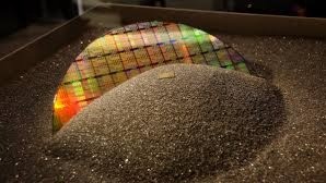
3. Wafer Slicing and Preparation
– The silicon ingot is sliced into thin discs called wafers, typically 200–300 micrometers thick.
– Wafers are polished to a mirror finish with atomic-level smoothness.
– After polishing, wafers undergo rigorous cleaning to remove any dust or contaminants that could ruin the chips.
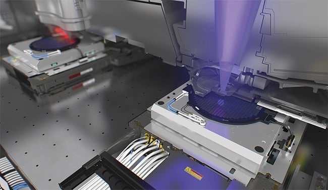
4. Photolithography: Drawing Circuits with Light
Here the magic begins:
– A layer of photoresist (light-sensitive chemical) is applied on the wafer.
– Using photolithography, ultraviolet light is projected through masks that contain circuit patterns.
– The exposed photoresist changes chemically, allowing selective removal.
– This process is repeated layer by layer, building the complex 3D structure of a microchip.
5. Etching and Doping: Sculpting Electrical Pathways
– Etching removes unwanted silicon or materials, shaping tiny transistor structures.
– Doping introduces impurities (like phosphorus or boron) to change the electrical properties of silicon in specific areas.
– These processes create the billions of transistors and connections that allow chips to function.
6. Testing, Cutting, and Packaging
– After fabrication, wafers undergo testing to identify defective chips.
– Functional chips are carefully cut (diced) from the wafer.
– Each chip is then packaged with protective casings and connectors.
– Packaged chips are ready to be installed in devices, powering everything from cars to phones.
Conclusion
The journey from simple sand to an advanced silicon chip is a triumph of human engineering and science. It involves transforming abundant raw materials into the heart of modern technology, enabling the digital revolution we rely on every day.

1 comment